File:Gerber-layers-example.png
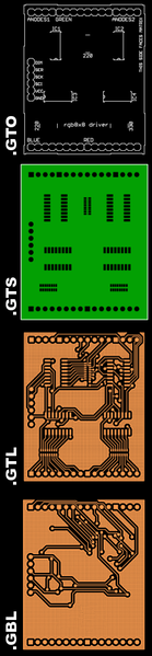
Size of this preview: 139 × 599 pixels. Other resolution: 232 × 1,000 pixels.
Original file (232 × 1,000 pixels, file size: 157 KB, MIME type: image/png)
Captions
Captions
Add a one-line explanation of what this file represents
| Description | Board design and Gerber file format image |
| Date | |
| Source | en.wikipedia.org/..Gerber-layers-example.png |
| Author | en:User:Halley |
| Permission (Reusing this file) |
Public domain |
| Other versions |
 |
Summary edit
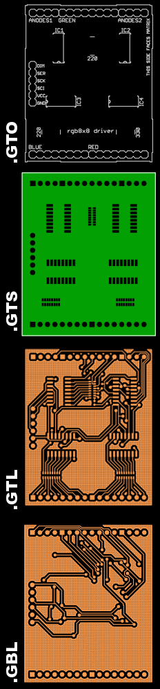
Board design and Gerber file format image created by Ed Halley, custom for Wikipedia article Gerber File.
Example Gerber layers, showing:
- .GTO file describes the top overlay (silkscreening to document the parts)
- .GTS file describes the top solder resist (a protective film to avoid stray solder)
- .GTL file describes the top layer copper traces (the rest is etched away)
- .GBL file describes the bottom layer copper traces of a printed circuit board.
Not shown: any silkscreening or solder resist on the bottom of the board, and a definition of all drill sizes and locations. Some designs may also have more copper layers sandwiched between boards.
Licensing edit
| I, the copyright holder of this work, release this work into the public domain. This applies worldwide. In some countries this may not be legally possible; if so: I grant anyone the right to use this work for any purpose, without any conditions, unless such conditions are required by law. |
File history
Click on a date/time to view the file as it appeared at that time.
| Date/Time | Thumbnail | Dimensions | User | Comment | |
|---|---|---|---|---|---|
| current | 16:53, 12 January 2010 | 232 × 1,000 (157 KB) | Bitsrc (talk | contribs) | {{Information |Description=Board design and Gerber file format image |Source=[http://en.wikipedia.org/wiki/File:Gerber-layers-example.png en.wikipedia.org/..Gerber-layers-example.png] |Date=19:47, 8 February 2009 |Author=en:User:Halley |Permission=Pu |
You cannot overwrite this file.
File usage on Commons
There are no pages that use this file.
File usage on other wikis
The following other wikis use this file:
- Usage on da.wikipedia.org
- Usage on ja.wikipedia.org
- Usage on sv.wikipedia.org