File:High-k.svg

Size of this PNG preview of this SVG file: 401 × 235 pixels. Other resolutions: 320 × 188 pixels | 640 × 375 pixels | 1,024 × 600 pixels | 1,280 × 750 pixels | 2,560 × 1,500 pixels.
Original file (SVG file, nominally 401 × 235 pixels, file size: 8 KB)
Captions
Captions
Add a one-line explanation of what this file represents
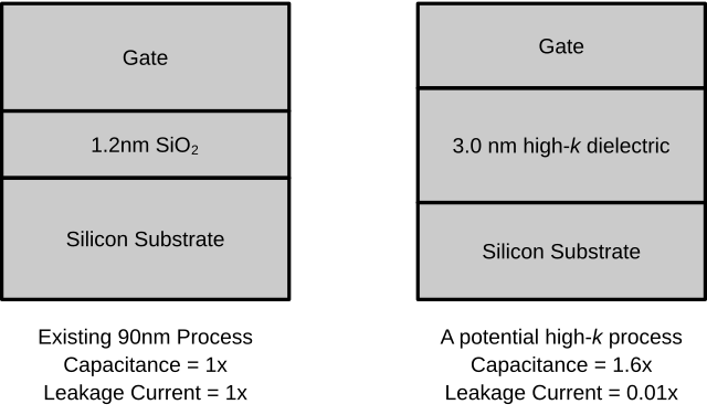
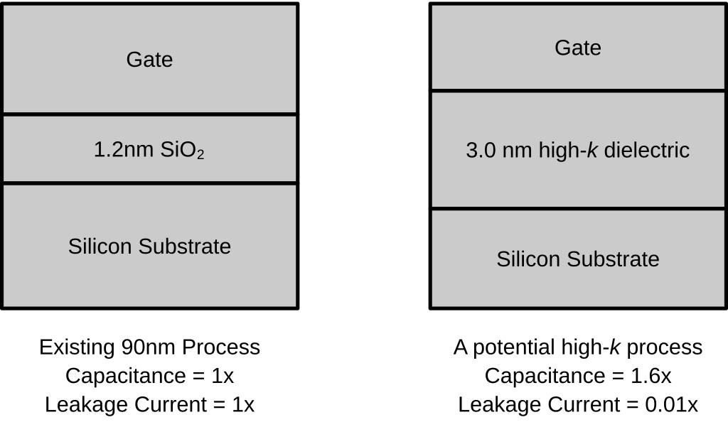
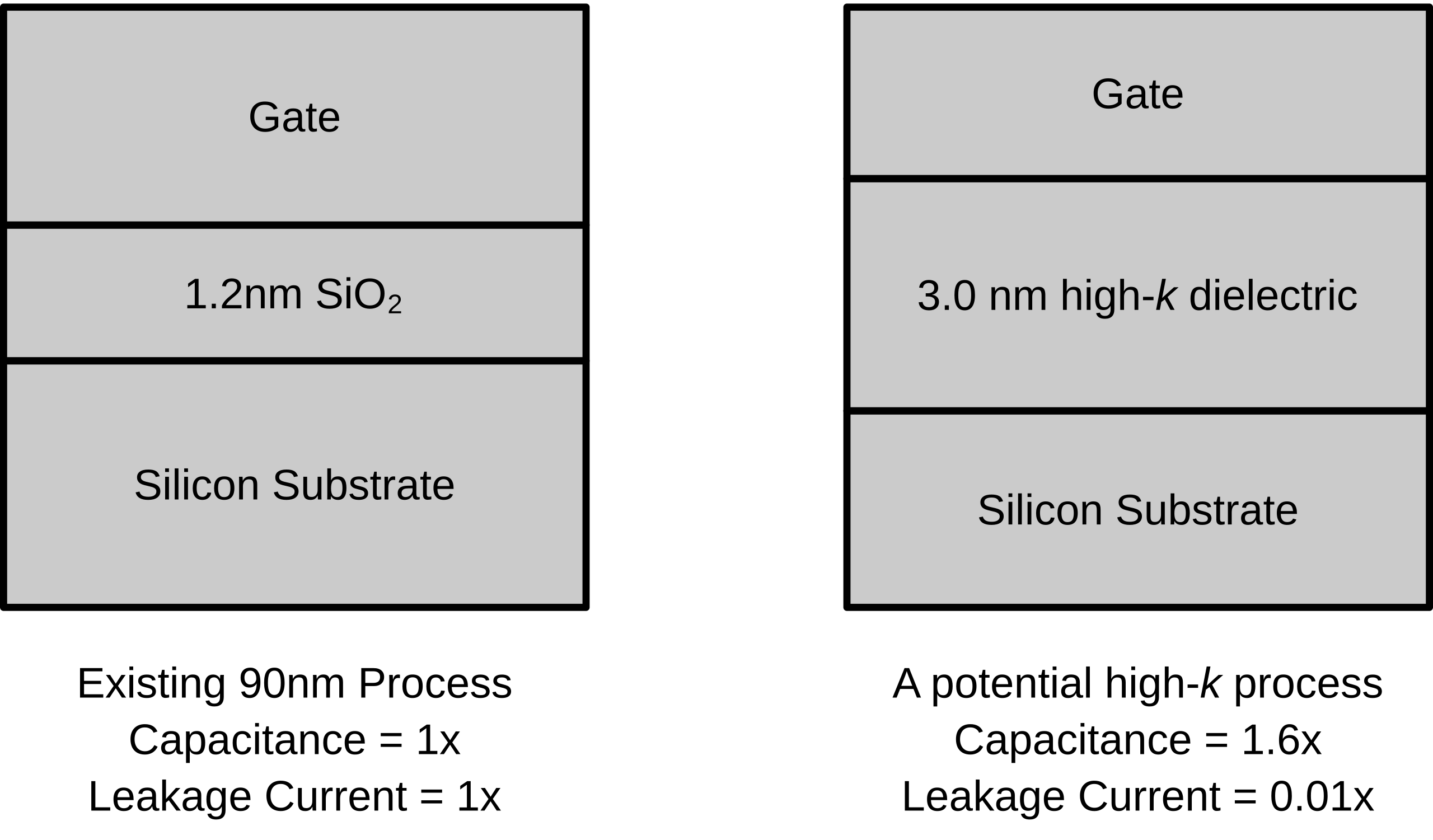
| Description | Comparison of high-k dielectric structure with conventional silicon dioxide gate dielectric. Schematic is my graphical representation of an idea in the presentation by G. E. Moore, Intel Inc. | ||||||||
| Date | 2006-01-05, 2008-01-14 | ||||||||
| Source | File:High-k.png | ||||||||
| Author | en:User:Anoopm, traced by User:Stannered | ||||||||
| Permission (Reusing this file) |
Anoopm at the English-language Wikipedia, the copyright holder of this work, hereby publishes it under the following license:
|
||||||||
| Other versions |
Derivative works of this file: Common SiO2 vs high-k gate stack (DE).svg File:High-k.png |

.svg)
File history
Click on a date/time to view the file as it appeared at that time.
| Date/Time | Thumbnail | Dimensions | User | Comment | |
|---|---|---|---|---|---|
| current | 18:14, 14 January 2008 | | 401 × 235 (8 KB) | Stannered (talk | contribs) | {{Information |Description=Comparison of high-k dielectric structure with conventional silicon dioxide gate dielectric. Schematic is my graphical representation of an idea in the presentation by G. E. Moore, Intel Inc. |Source=en:Image:High-k.png |Da |
You cannot overwrite this file.
File usage on Commons
The following 2 pages use this file:
File usage on other wikis
The following other wikis use this file:
- Usage on en.wikipedia.org
- Usage on en.wikiversity.org
- Usage on fa.wikipedia.org
- Usage on ja.wikipedia.org
- Usage on ru.wikipedia.org
- Usage on uk.wikipedia.org