File:Optoisolator Pinout.svg

Size of this PNG preview of this SVG file: 250 × 150 pixels. Other resolutions: 320 × 192 pixels | 640 × 384 pixels | 1,024 × 614 pixels | 1,280 × 768 pixels | 2,560 × 1,536 pixels.
Original file (SVG file, nominally 250 × 150 pixels, file size: 16 KB)
Captions
Captions
Add a one-line explanation of what this file represents
| Description |
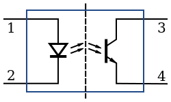
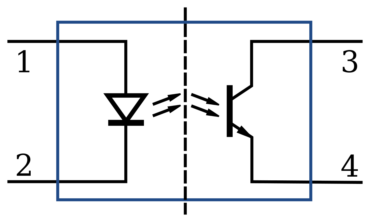
English: A schematic pinout of an extremely simple opto-isolator device. Often diode and transistor protection and/or amplification will be added. The dashed line in the centre represents to isolation barrer, over which no electrical contact can be permitted. |
||
| Date | |||
| Source | Own work | ||
| Author | Inductiveload | ||
| Permission (Reusing this file) |
|
||
| Other versions |
|


File history
Click on a date/time to view the file as it appeared at that time.
| Date/Time | Thumbnail | Dimensions | User | Comment | |
|---|---|---|---|---|---|
| current | 04:15, 19 November 2008 | | 250 × 150 (16 KB) | Inductiveload (talk | contribs) | {{Information |Description={{en|1=A schematic pinout of an extremely simple opto-isolator device. Often diode and transistor protection and/or amplification will be added. The dashed line in the centre represents to isolation barrer, over which no electri |
You cannot overwrite this file.
File usage on Commons
The following 5 pages use this file:
File usage on other wikis
The following other wikis use this file:
- Usage on bg.wikipedia.org
- Usage on ca.wikipedia.org
- Usage on de.wikipedia.org
- Usage on en.wikipedia.org
- Usage on es.wikipedia.org
- Usage on et.wikipedia.org
- Usage on eu.wikipedia.org
- Usage on fa.wikipedia.org
- Usage on fi.wikipedia.org
- Usage on fr.wikipedia.org
- Usage on hi.wikipedia.org
- Usage on it.wikipedia.org
- Usage on ja.wikipedia.org
- Usage on pl.wikipedia.org
- Usage on ro.wikipedia.org
- Usage on sv.wikipedia.org
- Usage on uk.wikipedia.org
- Usage on vi.wikipedia.org
- Usage on vi.wikibooks.org
- Usage on zh.wikipedia.org