File:(Geometry of Nature) Геометрія природи.jpg
Size of this preview: 800 × 600 pixels. Other resolutions: 320 × 240 pixels | 640 × 480 pixels | 1,024 × 768 pixels | 1,280 × 960 pixels | 1,700 × 1,275 pixels.
Original file (1,700 × 1,275 pixels, file size: 2.74 MB, MIME type: image/jpeg)
Captions
Captions
Add a one-line explanation of what this file represents
Summary edit
_%D0%93%D0%B5%D0%BE%D0%BC%D0%B5%D1%82%D1%80%D1%96%D1%8F_%D0%BF%D1%80%D0%B8%D1%80%D0%BE%D0%B4%D0%B8.jpg&action=edit§ion=1)
| Description |
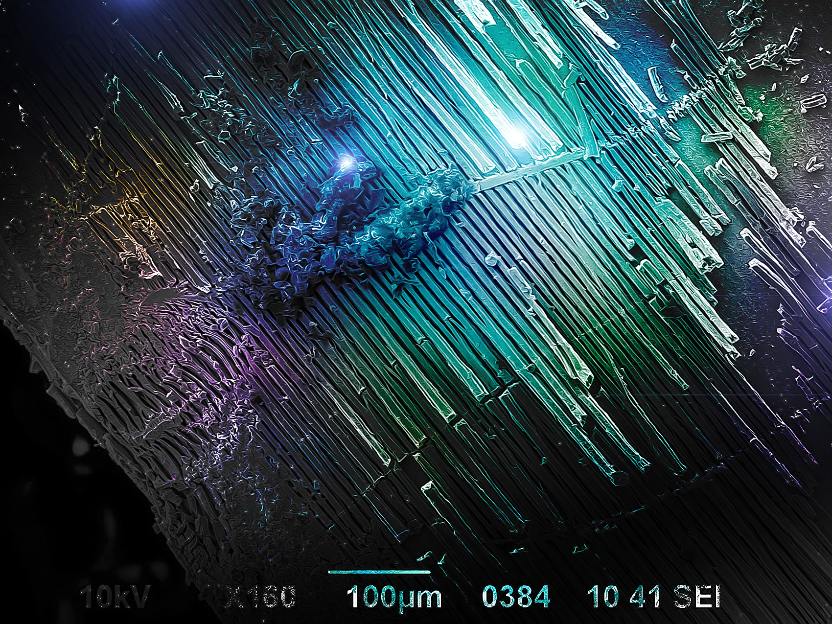
Українська: Зображення морфології текстурованої пластини фосфіду індію. Фотографії наноструктур було отримано на растровому електронному мікроскопі JSM-6490 дослідниками Бердянського державного педагогічного університету. Збільшення у 160 разів. Фосфід індію (InP) має великі перспективи широкого промислового виробництва. На основі фосфіду індію створюються польові транзистори і інші НВЧ прилади. Монокристалічні пластини InP використовуються в якості підкладок для вирощування різних гетероструктур, на основі яких створюються ефективні джерела випромінювання (інжекційні лазери, світлодіоди) і швидкодіючі фотоприймачі для систем волоконно-оптичних ліній зв'язку. Фосфід індію перспективний для розробки надшвидких інтегральних схем. На сьогоднішній день InP є найбільш вірогідним матеріалом для масового виробництва ІС. Не можна не згадати про зростаючий інтерес до пористого фосфіду індію, який має незвичайні оптичні та електричні властивостями в порівнянні з монокристалічний InP. Такі структури можуть знайти застосування при виготовленні сенсорів (так як їх чутливість залежить від площі поверхні) та сонячних батарей (можливість накопичення рекордної кількості енергії). English: The image of the morphology of the textured InP plate. Photos of nanostructures were obtained in scanning electron microscope JSM-6490 by the researchers of Berdyansk State Pedagogical University. Increased 160 times. Indium phosphide (InP) has great prospects of wide industrial production. Field-effect transistors and other microwave devices are manufactured based on InP. Monocrystalline InP plates are used as substrates for the growth of different heterostructures, which are the basis of effective radiation sources (injection lasers, light-emitting diodes) and high-speed photodetectors for the systems of fiber optic communication lines. InP is promising for the development of super-high-speed integrated circuits. Presently InP is the most probable material for the mass production of integrated circuits. It is impossible not to mention about the growing interest in porous InP, which has unusual optical and electrical properties in comparison with the monocrystalline InP. Such structures can find application in sensor (since their sensitivity depends on the surface area) and solar cell (possibility of the accumulation of a record amount of energy) manufacturing. |
| Date | |
| Source | Own work |
| Author | Яна Сычикова, Ковачев Сергей |
Licensing edit
_%D0%93%D0%B5%D0%BE%D0%BC%D0%B5%D1%82%D1%80%D1%96%D1%8F_%D0%BF%D1%80%D0%B8%D1%80%D0%BE%D0%B4%D0%B8.jpg&action=edit§ion=2)
I, the copyright holder of this work, hereby publish it under the following license:
This file is licensed under the Creative Commons Attribution-Share Alike 4.0 International license.
- You are free:
- to share – to copy, distribute and transmit the work
- to remix – to adapt the work
- Under the following conditions:
- attribution – You must give appropriate credit, provide a link to the license, and indicate if changes were made. You may do so in any reasonable manner, but not in any way that suggests the licensor endorses you or your use.
- share alike – If you remix, transform, or build upon the material, you must distribute your contributions under the same or compatible license as the original.
| This image was uploaded as part of European Science Photo Competition 2015. |
File history
Click on a date/time to view the file as it appeared at that time.
| Date/Time | Thumbnail | Dimensions | User | Comment | |
|---|---|---|---|---|---|
| current | 17:32, 30 October 2015 | | 1,700 × 1,275 (2.74 MB) | Yana Sychikova (talk | contribs) | User created page with UploadWizard |
You cannot overwrite this file.
File usage on Commons
There are no pages that use this file.
File usage on other wikis
The following other wikis use this file:
- Usage on be-tarask.wikipedia.org
- Usage on uk.wikipedia.org
- Usage on www.wikidata.org
_Геометрія_природи.jpg&oldid=733979720)