File:Surface MOCVD films defects.jpg

Size of this preview: 800 × 600 pixels. Other resolutions: 320 × 240 pixels | 640 × 480 pixels | 1,024 × 768 pixels | 1,280 × 960 pixels | 2,560 × 1,920 pixels.
Original file (2,560 × 1,920 pixels, file size: 418 KB, MIME type: image/jpeg)
Captions
Captions
Add a one-line explanation of what this file represents
Summary
edit
| Description |
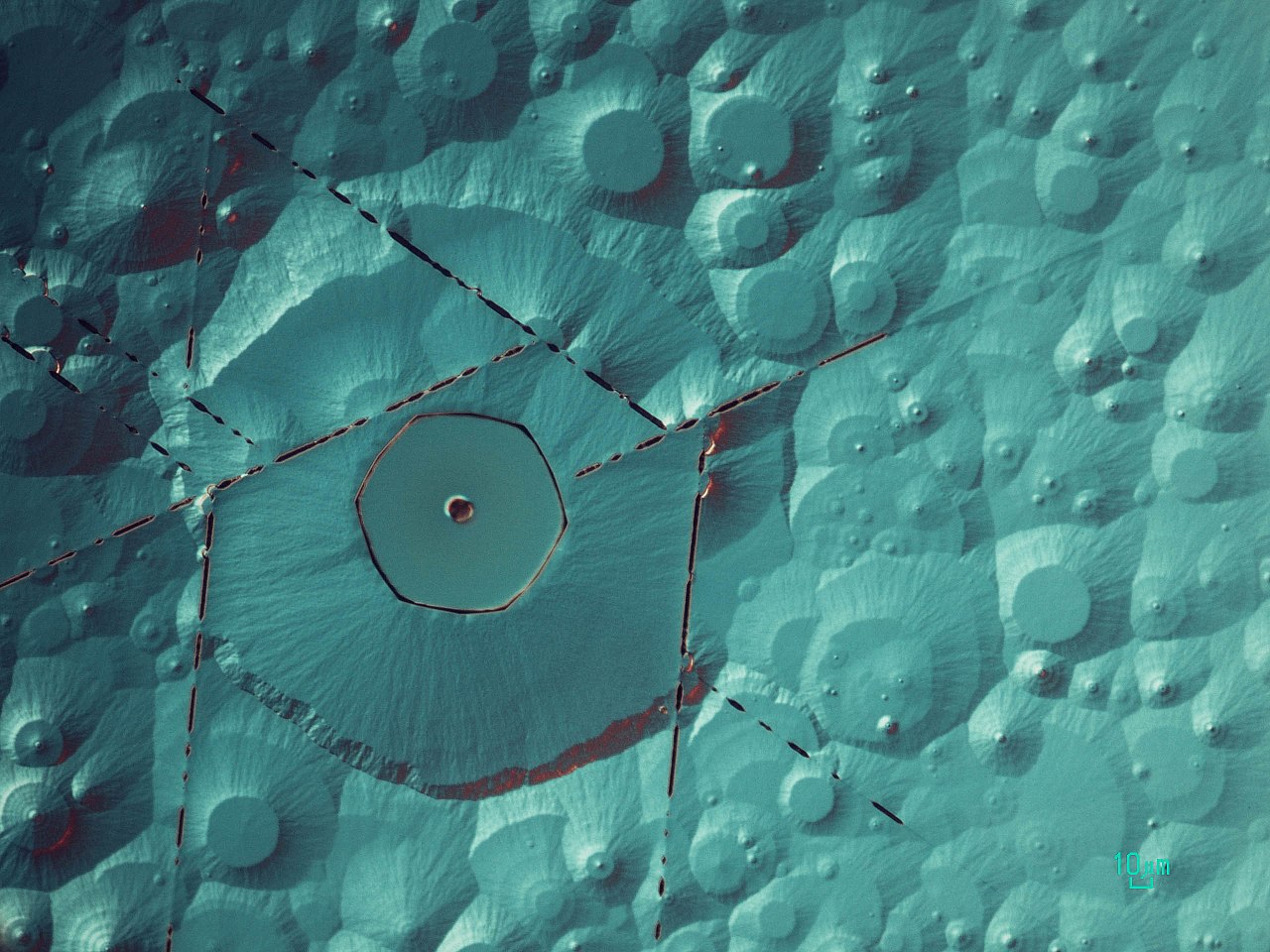
English: During the thin film deposition by MOCVD it is possible to form a film with small lattice constant on film with big one. In this case upper film will face tensile stress and will seek a way to get rid of it. Some ways of making it is: to growth not as a single sheet, but as a small sheets, to form cracks and holes. This image shows all kind of ways nitride film used to relieve stress and not-to-become a heterostructure for High Electron Mobility Transistor. The central part takes the form of a hexagon in accordance with the structure of the unit cell of the material. |
| Date | |
| Source | Own work |
| Author | Evavilova |
Licensing
edit
I, the copyright holder of this work, hereby publish it under the following license:
This file is licensed under the Creative Commons Attribution-Share Alike 4.0 International license.
- You are free:
- to share – to copy, distribute and transmit the work
- to remix – to adapt the work
- Under the following conditions:
- attribution – You must give appropriate credit, provide a link to the license, and indicate if changes were made. You may do so in any reasonable manner, but not in any way that suggests the licensor endorses you or your use.
- share alike – If you remix, transform, or build upon the material, you must distribute your contributions under the same or compatible license as the original.
| This image was uploaded as part of Wiki Science Competition 2017. |
File history
Click on a date/time to view the file as it appeared at that time.
| Date/Time | Thumbnail | Dimensions | User | Comment | |
|---|---|---|---|---|---|
| current | 10:33, 12 December 2017 | | 2,560 × 1,920 (418 KB) | Evavilova (talk | contribs) | User created page with UploadWizard |
You cannot overwrite this file.
File usage on Commons
There are no pages that use this file.