File:Tesla Autopilot HW2.5 and Infotainment Boards (50938493268).jpg

Original file (3,574 × 3,567 pixels, file size: 4.81 MB, MIME type: image/jpeg)
Captions
Captions
Summary edit
| Description |
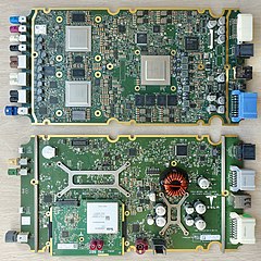
Given all the talk of automotive semiconductor shortages, I was curious to investigate the Tesla Autopilot module to which we have trusted our lives these past years. Here is a peek into the Model 3 HW2.5 module, from VIN0005. What we found: A magic box with liquid cooling tubes dripping a blue fluid. Inside are two circuit boards with thermal paste (grey and pink) connecting the processors on each board to the metal cooling plate that runs through the center. Tesla designed a custom liquid-cooled dual-computing platform with the Autopilot ECU and Infotainment MCU on two boards in the same module. There are two Nvidia Parker SoCs, one Nvidia Pascal GPU and one Infineon TriCore CPU. The autopilot ECU board has 4,681 components. It also has an Intel Atom processor, NXP and Infineon for the microcontrollers, Micron Technology, Samsung and SK Hynix memory and STMicroelectronics audio amplifiers. For the circuit boards, I’ll add descriptions of major parts, and feel free to add more part IDs to them. Top Board: Autopilot ECU with 4,681 components (mostly surface mount capacitors and resistors) •Upper left in White: <a href="https://www.u-blox.com/en/product/neo-m8l-series" rel="noreferrer nofollow">U-Blox</a> ADR Navigation chip with GNSS and sensors. •3 Big Silver squares: The NVIDIA chip package (2 Parker SoCs on left + 1 Pascal GPU to right). The Infineon TriCore CPU is near the top right corner of the GPU. •Colored connectors on left, starting from the top: GPS RF, BackupCam, SelfieCam, Main Cam, Repeaters, B-Pillar Cams, Front Cams, Video Out Bottom Board: Infotainment MCU (faces away from heat sink) •The big white chip on the cellular daughter card on the bottom is the <a href="https://www.telit.com/press-release/telit-achieves-att-certification-of-300-mbps-lte-advanced-automotive-grade-module/" rel="noreferrer nofollow">Telit</a> LE940B6-NA chip for 300MBps LTE connectivity. The SIM card is on the backside. •The big silver caps and inductor on the right are part of the audio amp • I see six debug ports (jumper, USB) that may just be just the early units (+5 more JTAG ports on backside of the NVIDIA board) |
| Date | |
| Source | Tesla Autopilot HW2.5 and Infotainment Boards |
| Author | Steve Jurvetson from Los Altos, USA |
| Other versions |
_(cropped)_Telit_LE940B6-NA.jpg)
_(cropped)_GP106-510.jpg)
.jpg&action=edit§ion=1)
Licensing edit
.jpg&action=edit§ion=2)
- You are free:
- to share – to copy, distribute and transmit the work
- to remix – to adapt the work
- Under the following conditions:
- attribution – You must give appropriate credit, provide a link to the license, and indicate if changes were made. You may do so in any reasonable manner, but not in any way that suggests the licensor endorses you or your use.
| This image was originally posted to Flickr by jurvetson at https://flickr.com/photos/44124348109@N01/50938493268. It was reviewed on 10 May 2021 by FlickreviewR 2 and was confirmed to be licensed under the terms of the cc-by-2.0. |
File history
Click on a date/time to view the file as it appeared at that time.
| Date/Time | Thumbnail | Dimensions | User | Comment | |
|---|---|---|---|---|---|
| current | 08:39, 10 May 2021 | | 3,574 × 3,567 (4.81 MB) | Sentinel user (talk | contribs) | Transferred from Flickr via #flickr2commons |
You cannot overwrite this file.
File usage on Commons
The following 3 pages use this file:
File usage on other wikis
The following other wikis use this file:
- Usage on en.wikipedia.org
- Usage on es.wikipedia.org
- Usage on fa.wikipedia.org
- Usage on ja.wikipedia.org
.jpg&oldid=646025274)